

In the rapidly evolving world of electronics manufacturing, PCB Design Services have become more vital than ever. As technological complexity rises and miniaturization becomes standard, the processes behind printed circuit board (PCB) assembly and soldering are undergoing significant transformation. In 2025, manufacturers are shifting towards automation, precision, and sustainability to keep pace with new device demands and regulatory expectations. Understanding these trends helps design engineers, assemblers, and manufacturers stay competitive and forward-looking.
This article explores the modern trends shaping PCB assembly and soldering methods, from evolving surface-mount technologies to eco-friendly soldering techniques and automated quality assurance.
Printed circuit board assembly (PCBA) is no longer a one-size-fits-all process. It has grown into a diverse and technology-driven field with solutions tailored to specific applications, industries, and design complexities. In 2025, the focus has shifted toward flexibility, speed, and reliability.
SMT continues to dominate PCB assembly due to its space-saving benefits and compatibility with automated processes. Advanced placement machines now handle even the smallest components (like 01005 packages) with increased accuracy. These machines are integrated with AI-powered vision systems, reducing error margins and increasing throughput.
The demand for smaller, faster, and more functional devices is pushing designers towards HDI PCBs. These boards require precise assembly processes, as they incorporate microvias, fine-pitch components, and thinner materials. Soldering techniques also need to adapt to prevent damage during reflow or wave soldering.
With the rise of miniaturized boards and complex solder joints, automated inspection systems are no longer optional. AOI, Automated X-ray Inspection (AXI), and solder paste inspection (SPI) are now standard across PCB assembly lines. These tools provide real-time feedback and enable predictive maintenance, reducing downtime and enhancing yield.
In parallel, smart factory integration allows for centralized control, traceability, and data-driven process refinement—making inspection tools part of the broader Industry 4.0 framework.
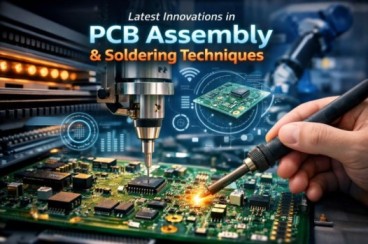
Soldering, once a manual and operator-dependent process, has evolved into a highly automated and data-driven operation focused on repeatability, safety, and long-term reliability. As electronic designs become denser and more complex, newer soldering techniques and advanced materials are being introduced to meet tighter tolerances and higher performance expectations.
1. Reflow Soldering with Controlled Profiling
Reflow soldering remains the dominant method for surface-mount technology, but recent advancements have significantly improved its effectiveness. In 2025, multi-zone reflow ovens are increasingly used to create customized thermal profiles for different sections of a single PCB. This capability is especially important for hybrid assemblies where components have varying thermal sensitivities.
To further protect delicate components, manufacturers are adopting low-temperature solder pastes and nitrogen-controlled environments. These measures reduce oxidation, minimize thermal shock, and ensure strong, consistent solder joints without compromising component integrity or board reliability.
2. Selective Soldering for Mixed Assemblies
Mixed-technology PCBs that combine SMT and through-hole components continue to play a critical role in many industries. Selective soldering has emerged as a preferred solution, offering greater control compared to traditional wave soldering. By targeting only required joints, selective soldering reduces unnecessary heat exposure and improves overall solder quality.
Modern selective soldering systems feature programmable solder paths, precise flux deposition, and real-time process monitoring. These capabilities make them well suited for high-reliability applications in automotive, aerospace, industrial, and medical electronics, where consistency and defect prevention are essential.
3. Advanced Solder Materials and Process Control
In addition to equipment improvements, innovation in solder alloys is driving better performance. Lead-free and low-silver alloys are being optimized for improved wetting, reduced voiding, and enhanced mechanical strength. Combined with real-time thermal monitoring and closed-loop feedback systems, these materials help manufacturers maintain tight process control and deliver highly reliable PCB assemblies.
As soldering technologies continue to advance, precision and reliability will remain central to achieving durable, high-performance electronic products in demanding operating environments.
Global regulations and sustainability goals are pushing the industry towards lead-free and halogen-free soldering options. Alloys such as SAC305 (Tin-Silver-Copper) and low-silver variants are increasingly preferred due to compliance with RoHS and REACH directives.
Moreover, water-soluble fluxes and VOC-free cleaning processes are being integrated to reduce harmful emissions and waste in PCB manufacturing plants.
For more information on foundational and evolving techniques, refer to this detailed blog on PCB assembly technologies and soldering techniques, which outlines practical considerations and tools for implementing the latest processes in real-world assembly lines.
A significant trend in 2025 is the tight integration between PCB Design Services and assembly requirements. Engineers are adopting Design for Manufacturability (DFM) principles early in the design cycle to reduce rework, lower costs, and improve time-to-market.
This includes:
This collaborative approach ensures that boards are not just functional in theory but practical to assemble and solder reliably.
AI has begun to revolutionize multiple stages of PCB assembly, particularly in:
In 2025, companies offering PCB Design Services are increasingly expected to integrate these AI tools into both design validation and production preparation.
While innovation in PCB assembly is impressive, several challenges persist, especially regarding component shortages and the increasing complexity of multilayer and flexible PCBs.
Some areas to watch:
Modern trends in PCB assembly and soldering methods reflect a broader shift toward higher precision, advanced automation, and stronger environmental responsibility across the electronics industry. Manufacturers are increasingly adopting intelligent inspection systems, AI-driven quality checks, selective soldering processes, and low-temperature, lead-free materials to improve consistency while reducing defects and energy consumption. These advancements not only enhance product reliability but also support sustainable manufacturing practices and faster production cycles.
For businesses and engineers offering or seeking PCB Design Services, staying aligned with these evolving techniques is no longer optional. A clear understanding of modern assembly and soldering innovations enables the delivery of highly reliable, scalable, and cost-efficient electronic solutions. As technology continues to evolve, assembly and soldering will remain core pillars in achieving next-generation performance, miniaturization, and long-term product durability.
© 2025 Crivva - Hosted by Airy Hosting Managed Website Hosting.


